


Supported by over 100 partner factories with over 200
production lines, PCBAI provides customers with turn-key manufacturing services for
small and large batch volumes


PCBAI Serves Full Range of Commercial and Industrial Categories by Leveraging Our Flexible Manufacturing Network
Industrial Control


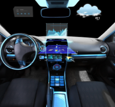
Automobile Manufacturing

Medical Electronics

Consumer Electronics

Network Communication


AI

Comprehensive Factory Audit System
The review covers 8 major items and 165 other detailed items covering personnel, equipment, material, process, environment,
system preparation and implementation.Under Evaluation Content, capitalize the first letter of Quality control, Process control, etc.
Four KPI Review Items of the Factory


Evaluation Content
ISO9001:2015
IATF16949:2016
ANSI/ESD S20.20
IPC-J-STD-033
ISO9001:2015
IATF16949:2016
IPC-A-610H
(resistance assembly acceptance)
ISO9001:2015
IATF16949:2016
IPC-J-STD-001
(welding requirements for electrical and electronic components)
IPC-7711/21
(rework, modification and maintenance of electronic components)
ISO9001:2015
IATF16949:2016
ISO9001:2015
IATF16949:2016
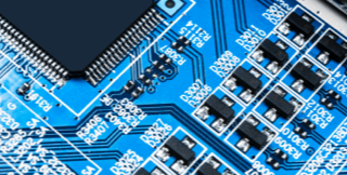
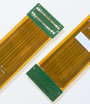
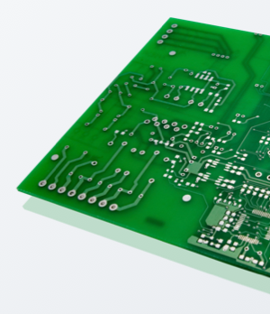
PCB Board Production
Single And Two-sided, Four Layers, Process, Copper Substrate, Thick Copper Plate Buried Hole/HDI, Class A Board, Strict Quality Control Ensured
Through 36 Processes
two sides 0.2-3.0mm, multiple layers more than
0.4mm
single-sided board≤1.0%, two-sided
board≤0.70%, multilayer board≤0.50%
0.15mm
0.1mm
10:1
5mil
0.2mm
0.3mm
±0.3mm
±0.1mm
0.076mm or 3mil
0.127mm
0.076mm(3mil),minimum window opening of
bonding pad:0.076mm
electricity, tin spray, gold immersion,
tin immersion, silver immersion, OSP

PCB Assembly Service


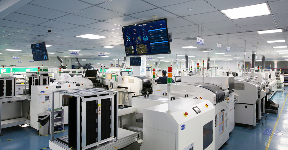

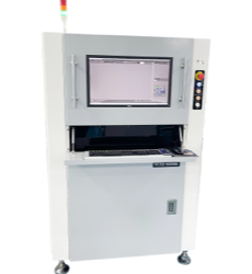
AOI
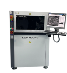
SPI
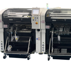
SMT
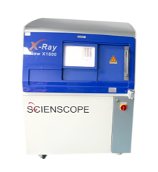
X-RAY
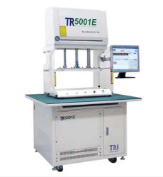
ICT


Get Started with PCBAI
Allied with hundreds of factories providing strict quality control and service gurantee