
Full Quotation and Manufacturing Services by Uploading Your Design Files
Transparent manufacturing service from technical consultation to product delivery.
Technical consultation-> design optimization-> material purchase-> PCB original equipment manufacturing-> PCB SMT service-> product testing-> product assembly-> delivery of finished product
Reduce Your Production Costs and Shorten Your Development Cycle with Our Early Design Optimization Services
Based on our rich development experience and taking the manufacturing process into account, we can make suggestions for component selection, design optimisation and cost reduction.


Complete Material Procurement for BOM
Supply Chain Support
>Large-scale material procurement platform
The in-house material procurement platform has more than 100 million SKU of data, and serves nearly 100,000 enterprises, with annual sales of $630M+ USD.
Our scale provides customers with favorable prices.
Our promise: all products are genuine; customers will be compensated tenfold for any counterfeit products.
>A large selection of low-cost products
1000+ high-quality cooperative suppliers.
Products are divided into various categories, including discrete devices, optoelectronic devices and integrated IC chips.
Short delivery time for spot commodities.
Procurement Service
>Efficient and transparent procurement service.
Personalized service from our professional staff will track the procurement process with you every step of the way.
We will help you purchase all the materials with a complete BOM and one-stop procurement, saving you time and stress.
>Material management service
You will receive alerts and notifications in real time based on our analysis of customer demand cycles and global supply chains.
Customers with periodic reinvestment and multiple reorders can also enjoy an advance material preparation service. Full time service personnel will assist customers in managing their material inventory and give appropriate optimization suggestions.
PCB Manufacturing Capability
Finished board thickness
two sides 0.2-3.0mm, multiple layers more than 0.4mm
Minimum solder mask bridge
5mil
Warpage size
single-sided board≤1.0%, two-sided board≤0.70%, multilayer board≤0.50%
Distance between copper sheet and board edge
0.2mm
Minimum aperture of mechanical hole
0.15mm
Distance between hole edge and wire edge
0.3mm
Minimum aperture for laser drilling
0.1mm
Forming dimension tolerance
±0.13mm
Ratio of board thickness to aperture
10:1
V-CUT alignment accuracy
±0.1mm
Minimum width/gap of wire
0.076mm or 3mil
Minimum marked font
0.127mm
Minimum width of single side for welded ring
0.076mm(3mil),minimum window opening of bonding pad:0.076mm
Surface treatment
electricity, tin spray, gold immersion, tin immersion, silver immersion, OSP

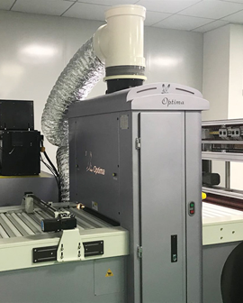
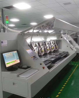
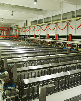
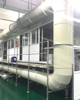


PCB SMT Service
Advanced production equipment
Standardized mounting process
Automatic testing process
Systematic quality management
Test & Assembly
We apply routine tests such as ICT and FCT to find any defects in the manufacturing process and verify all boards are functioning correctly. Equipment and test procedures are used to detect the functional status of the finished products according to the specific customer requirements. We can also assemble and test different parts within the BOM based on customer drawings to meet their product requirements and provide a more comprehensive service.